“We can contribute a lot to the global technology field with the high level of expertise available in Austria”
The global Siemens technology field Integrated Circuits and Electronics is headed by Herbert Taucher from the research unit in Vienna. Two of nine research groups involved are also based in Austria. An interview about the combination of hardware and software, supply chains, AI, sustainability and the central role of Siemens in chip development on the global market.
You have been in charge of the global Siemens technology field Integrated Circuits and Electronics (ICE) since the beginning of 2023. What are the topics in this research area? We deal with integrated circuits (ICs) and printed circuit board-based electronics (PCBs). These are key technologies for most industries, which are essential for digitalization in particular. ICE covers design, verification and manufacturing through to the circular economy of ICs, PCBs and modules for various forms of electronics – such as digital and analog electronics, high-frequency electronics, photonics and MEMS (Micro-Electro-Mechanical Systems) technologies to realize a range of capabilities such as compute platforms, wired and wireless communications, sensors and actuators. Our research agenda also includes batteries — from cell production optimization to circular economy. ICE combines the relevant engineering and research disciplines and we work closely with the technology fields and universities that focus on software and system development and, of course, with the research groups in the various Siemens business units.
What does the organizational setup look like? ICE is one of eleven Siemens technology fields in the technology organization of our CTO Peter Körte and, in addition to two technology fields that have been managed from the USA for years, the only one that has its headquarters outside Germany. Nine teams – so-called research groups – work in five countries in the ICE technology field based in Vienna. There are four research groups in Germany, one in India, one in Romania, one in Portugal and two in Austria – namely the research groups “Electronics Design and Integrated Circuits” and “Electronics Communication & Radio Frequency”, i.e. high-frequency technology. In total, around 160 experts from a wide range of disciplines are driving the topics forward.
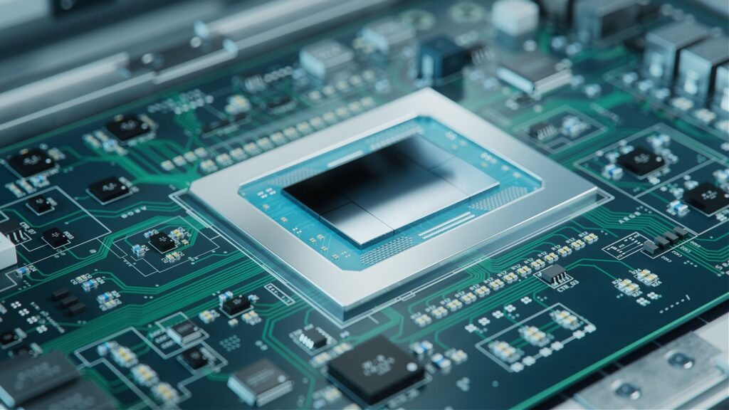
What is the significance of semiconductors for Siemens products? Almost all Siemens products consist of a combination of software and hardware. The optimal coordination of these two elements plays a key role, this is why hardware has always played a central role in Siemens’ strategy and will continue to do so. In the vast majority of cases, this hardware is based on electronics with embedded processors of various performance classes for executing the software. Siemens manufactures almost all of the electronics for these products itself at its own production sites. One of them is based in Vienna. Stable supply chains for ICs and electronic components in general are therefore extremely important for Siemens.
What is the situation in this respect? Although the situation has improved, there is still no sign of easing yet. It was a problem, that during the coronavirus pandemic, staff were unable to enter the factories and production came to a standstill.
And currently? There are currently capacity problems due to the very strong growth in demand on the market. Computing power-intensive AI applications such as large language models also make a significant contribution to this. The situation is therefore still very challenging, because we need stable supply chains for industrial products, usually for at least ten years. Every new chip production facility is essential for improving security of supply. We are not only talking about leading-edge production for the latest and smallest process structures, such as those required for all the chips in data centers and smartphones, but also for the widely used so-called legacy chips, i.e. chips that are manufactured in larger structure sizes and are very important for industry and the automotive sector.
What is the position of Siemens on a global level in the development of electronic components? Siemens recognized the importance of software tools for product development many years ago. An acquisition in 2007 laid the foundation for this. With the acquisition of Mentor Graphics in 2017 and subsequent acquisitions, the consistency of tools for the development of large complex systems down to the level of small electronic components such as chips was completed. At the end of 2020, the Mentor Graphics brand finally became Siemens EDA – Electronic Design Automation. We are one of the top 3 suppliers on the global market for development tools for chips and PCBs, i.e. printed circuit boards fitted with various electronic components. Siemens is also the only EDA provider with European roots among the top 3 providers.
“We are one of the top 3 suppliers on the global market for chip and PCB development tools. In addition, Siemens is the only EDA provider with European roots among the top 3 providers.”
Herbert Taucher, Technology Field Manager Integrated Circuits and Electronics
What can Siemens offer customers in the chip industry? We have a very extensive product portfolio for the chip industry. The EDA portfolio for chip design has already been mentioned. It covers all the steps involved in creating the blueprint for chips, and includes procedures for testing and diagnosing the manufactured chips. A large number of tools are required along the chip development process to ensure functional logical correctness, correct physical implementation and fast and complete testing of the manufactured chips. Siemens EDA is the technology and global market leader for some of the key steps in this development chain.
Are there also offers for the construction of chip production facilities? Yes, for the foundries, the portfolio ranges from tools for planning chip factories to products for the infrastructure of this production, like the supply of energy, liquids and gases, including automation and drive technology. In addition, Siemens products – both software and hardware – are essential components of the machines for the approximately 1,000 production process steps in the clean room of the foundry. Bear in mind that we support the semiconductor industry in achieving its sustainability goals with our holistic industry solutions geared towards sustainability in order to bring more sustainable chips onto the market.
Can you describe this aspect of sustainability in more detail? The chip industry is one of the biggest consumers of electrical energy and contributes accordingly to CO2 emissions. More than 60 elements from the periodic table are used in chip production and are further processed in the foundries in various process steps. However, chips contribute to sustainability in various dimensions.
What are those dimensions? Energy-efficient compute architectures are the first dimension. This means that certain chip microarchitectures are particularly efficient for certain classes of software and can run them particularly quickly or with particularly low power loss. Just as you think carefully about which software should run on a general purpose processing cluster or a GPU (graphics processing unit) cluster in a data center, you also consider which combination of these basic microarchitecture components should be implemented in a chip for a Siemens product.
Power semiconductors, which conduct and switch as efficiently as possible and should therefore have as little power loss as possible, and the low-power design form another dimension. The aim is to optimize chips and electronics for minimum energy consumption in order to maximize battery life, for example. This means, for example, that batteries for wireless sensor products only need to be replaced every few years and can be carried out as part of regular machine maintenance.
And finally: The chip in a product is, so to speak, the brain, that decisively determines how the product behaves in terms of efficiency. With intelligent control of the products by the software on the chips, the service life of the products can be increased and the product as a whole becomes more sustainable because it not only lasts longer but also generates less power loss. Digital twins also give us the opportunity to optimize the operation of the product with the chip installed even before physical production during development.
Quite a number of sustainability aspects. But that’s not all: when it comes to energy monitoring and optimization of all the process steps, we have a strong portfolio and a great deal of expertise to help producers understand and reduce their current CO2 footprint. At the end of last year, we launched a partnership with Intel with a number of initiatives, including the optimization of energy management and the reduction of the CO2 footprint along the entire value chain. As part of the cooperation, it will also be examined how energy consumption can be minimized, processes to reduce the consumption of natural raw materials can be further developed and the ecological footprint can be reduced.
What significance do the EU initiatives and those of other regions of the world in the chip sector have for your research activities? The relevant programs such as the EU Chips Act and comparable activities in the USA and other economic regions are key drivers for improving security of supply and innovation. These programs primarily address the establishment of ecosystems around chip development and production. Research, commercial suppliers and customers work together here. Siemens is a key partner both as a provider of EDA tools for chip development and manufacturing and infrastructure technology and as a purchaser of chips for widespread use in Siemens products. The main areas of research are AI-supported chip design methods, energy-efficient secure compute architectures and sustainability along the chip life cycle.
What role does AI play in chip development now and in the future? AI already plays an important role in chip development and this has now received an additional strong boost from large language models and generative AI technologies. On the one hand, AI is used to support and partially replace extremely computationally intensive analytical algorithms that do not scale appropriately in their execution time as the complexity of the chips increases; on the other hand, it is used in the form of chatbot-like functions as a co-pilot to support aspects such as development time, quality and productivity. A lot of research is being carried out into how generative AI and machine learning can contribute to more efficient chip development. The question is: How can these technologies be used so that experienced developers can carry out electronics or chip development even more effectively and quickly in the future, or less experienced developers can use AI-based assistance to implement significantly more challenging tasks at the level of experienced developers?
Are there any other research topics? The ICE teams in Austria are also involved in all the topics we are doing research, in collaboration with the other Siemens Technology research groups in Austria. With the high level of expertise available in Austria, we can contribute a great deal to the global technology field.
Research focus in the Integrated Circuits and Electronics (ICE) technology field
● Advanced Compute Architectures This is the composition of a chip’s computing capabilities from various microarchitectures tailored to the respective software. AI and GenAI as executable software require special capabilities from the chips they run on, in order to be executed efficiently. This ranges from special instruction extensions for processors and special accelerator architectures (Neural Processing Unit – NPU) to neuromorphic computing in the narrower sense, that is based on the functions of the human brain. However, real-time capable and functionally secure chips also require special compute architectures.
● Digital Twin for Electronics-based Systems This is about connecting the digital twin of a chip with the digital twin of a plant or system. The aim is to simulate not only the simplified behavior of a system itself, but also the detailed execution of the system’s software by the chip in this system. Digital twins of complex systems, such as an AMR (Autonomous Mobile Robot) in a production hall, with a level of detail down to the simulation of the execution of the software in the AMR for recording the environment and the movement of the AMR on a simulated model of the chip, open up completely new possibilities for the optimization of products in development through to the virtual commissioning of products in the customer environment.
● Novel wireless communication and sensing In addition to data transport, wireless communication can also perform other important tasks – such as using the technology to record the environment: In addition to the reliable exchange of information, localization in particular is a key function for flexible manufacturing. In many cases, this must also meet safety standards to protect life and limb. In addition, 5G and 6G for industrial applications as well as intelligent antenna solutions are key research priorities.
● AI, machine learning, generative AI for more efficient development (see interview, last answer)
Infobox:
Semiconductors, chips, printed circuit boards – what is what?
The term semiconductor as a group of elements in the periodic table with special conductive properties is also used colloquially as a broad umbrella term for chips. The demarcation is not sharp. The colloquial term semiconductor also refers to components with only two (diodes) or three (transistors, thyristors etc.) connections, for example. Chips are associated as components with a large number of connections. Chip and integrated circuit are synonyms. PCBs (Printed Circuit Boards) integrate the various electronic components into electronic systems, i.e. electronics. PCBs are composite materials consisting of epoxy resin and glass fiber fabric. These thin green sheets are coated with copper tracks and then stacked to create the 2 to 60-layer printed circuit boards. Resistors, capacitors, semiconductors (diodes, chips, …) and other electronic components are soldered onto them